Micro Parts Dominate Rapid Manufacturing
Rapid prototyping is exciting, but the real promise of additive fabrication is its potential for rapid manufacturing, or the volume manufacture of production parts. Due to the cost of RP systems and materials, and the slow build time of parts, rapid manufacturing is generally not yet feasible – except in the booming niche of micro additive fabrication. Micro RM has even higher systems and materials costs than standard rapid manufacturing, but with the ability to manufacture thousands of parts in a single build, the time per part is much less than other
Micro RP FineLine Prototyping looks similar to a standard rapid prototyping service bureau. Like other service companies, the North Carolina outfit will build you any size prototype using its eight stereolithography (SLA) machines, three 3D printers, and a single selective laser sintering (SLS) system. However, leveraging the experience of its president, the company does about 75 percent of its work in tiny parts. FineLine’s Rob Connelly assisted 3D Systems in the 1990s to refine a high-resolution SLA system. In 2001, he bought their first commercial one – the Viper. Over the years, he bought five more (In 2007, he bought their 500th one). The Viper, when used in high resolution mode, utilizes an 89 micron diameter ultra-violet laser to solidify the liquid photopolymer (as compared to a 254 micron diameter laser in standard mode) into feature sizes as small as 101 microns with an accuracy of ±50 microns. Max part size is a relatively roomy 254mm cubed. Connelly also uses special techniques, like reducing the amount of laser exposure, to allow for easy voiding of tiny non-cured areas. FineLine uses epoxy resins from 3D Systems and DSM Somos, including Nanotool, DMX, Prototherm, Watershed, and 9120. Seventy-five percent of the company’s mini work is for the medical industry, including microfluidic devices. “The business is growing nicely under any economic situation,” says Connelly. So is the size of orders. “We have found our volumes requested from customers have gone up over the past two years,” he says. FineLine has one customer who regularly places a 1,200-piece order. It takes about 3 days to fulfill the order for the 12mm square parts covered with small features, Connelly says. Micro Ceramic For a decade, CAM-LEM (Computer-Aided Manufacturing of Laminated Engineering Materials) has specialized in making small parts in ceramics for applications requiring high temperatures, electrical insulation, or chemical resistance. Using techniques from laminated object manufacturing (LOM), Ohio-based CAM-LEM uses a laser cut, stack, laminate, debind, sinter process that was originally developed at Case Western Reserve University. For most of its existence, CAM-LEM has helped to design and develop prototypes, only to have the parts be hard-tooled offshore. “It has been very disheartening,” says CAM-LEM Director Cameron Fordyce. “They reduce the tolerance, the draft has to be changed to Y, they send it overseas and have it injection molded.” That’s beginning to change, though. With more powerful computer chips in increasingly tighter confines, traditional cooling devices and heat sinks don’t do the job anymore. Semiconductor and LED microfluidic cooling systems made out of ceramic provide better chemical resistance and strength than plastic or silicon, and better strength and temperature resistance than glass. “700 or 800 degrees Celsius definitely reduces your options,” says Fordyce. Available ceramics include alumina, zirconia, silicon nitride, and zirconia-toughened alumina (ZTA). Metals such as 316L stainless are also available. CAM-LEM’s C1-100 System laser cuts and stacks .03 to 1.3mm thick tape with a powdered ceramic (or metal) and polymer binder mix. When the assembly is sintered, it is uniform and fully dense. Features to 50 microns are attainable. Typical part sizes range up to 200 x 150 x 150mm. CAM-LEM is working on tolerance-tightening improvements to its three systems, including refining the laser beam width and improving servo accuracy. “We are in the process of upgrading so we can get to higher production,” says Fordyce. Super Output Since 1996, Germany-based microTEC has developed a family of stereolithography-type technologies that take rapid manufacturing to the next level. Its RMPD-mask (Rapid Micro Product Development) systems can now produce one million parts per hour per system. In other words, using a 355mm mask, a 1 x 1 x 1mm component can be produced every microsecond in batch production. Besides higher precision than is possible with micro injection molding and the inherent flexibility of tooling-free production, microTEC has also developed a new solution for microelectronic heat dissipation. For use in MEMS (microelectromechanical systems), the company offers a microfluidic for cooling that doesn’t use pumps or any additional energy. Integrated on to a chip, tiny cooling pipes use capillary action to transport the condensate for evaporation. On its 10 machines, microTEC runs a range of UV curing materials, including epoxies, acrylics, and sol-gel materials. The company won’t give an exact figure for build precision, other than to say that it is in the micrometer range, and “sub-nanometer” surfaces are possible using their RPMD-nanoface technology. “Bestsellers at the moment are microfluidic chips, micro gears and other micro mechanical parts, high integrated nands, pressure sensors and optical components,” CEO Andrea Reinhardt tells RapidToday by email. “Customers are asking more and more for flexible units, with a trend for higher numbers. Millions we do, [the] next step is going into 100 million per part per year.” Like with conventional processes, there are significant price breaks at the higher volumes. According to the company’s standard price sheet, a 0.7mm diameter x 0.7mm high micro-gear costs US$35 each in quantity of 100, and US$.03 each in quantity of one million. Microscopic Assemblies One California firm operates in a different realm in terms of size and capability. Microfabrica (formerly MEMGen Corp.) not only works at a tinier level than most companies in this niche, the company also can build assemblies with dozens of independently working metal parts. Microfabrica’s proprietary electrochemical fabrication (EFAB) technology uses an additive/subtractive deposition/planarization process. For each layer, a structural metal and sacrificial metal are deposited, then planarized, or flattened, to a precise level. Once the build is complete, the sacrificial copper metal is removed by an etching process. Features smaller than 5 microns are possible, with 2 micron accuracy and repeatability. To attain these types of numbers, Microfabrica fabricates components and assemblies on a 100mm ceramic wafer substrate in a clean room, similar to semiconductor manufacturing. Unlike with most other rapid prototyping technologies, there is a tooling requirement – the photomasks used in fabrication. And so far, there are only two material options: Valloy-120, a nickel cobalt (Ni-Co) alloy that has mechanical properties that are similar to medical-grade stainless steel, and Edura-180, a rhodium (Rh) formulation that is almost as hard as ceramic and has high electrical conductivity. According to EFAB technology inventor and CTO Adam Cohen, Microfabrica has seen activity in medical products, but also microwave and millimeter-wave radio frequency (RF) devices, inertial and timing devices like used in safing and arming (fuzing) for defense work, and high accuracy probes for testing memory chips and microprocessors. (Cohen has an outsized reputation in the RP world – he led the development of 3D Systems’ SLA-250 stereolithography system, founded the Rapid Prototyping Report newsletter, co-founded Soligen Technologies, and holds 34 U.S. patents in RP and micromanufacturing.) Next up for Microfabrica is more expansion. “We have over 40 people and are growing quickly,” says Cohen. By the first or second quarter of 2009, the company plans to launch a new larger 150mm wafer system that will be used primarily for high-volume production runs. Additional Resources:
D-MEC Ltd. (Japan) PROFORM AG (Switzerland) Rapid Prototyping Lab at the University of Waterloo (Canada) microLS GmbH (Germany) Want to comment on this article? Visit our additive manufacturing forum. Want to read more? Visit our additive manufacturing archive. Originally published: July 2008
alternatives. Add to that the standard advantages of rapid prototyping – no tooling cost, the ability to create impossible-to-machine-or-mold geometries – and you have a compelling case. As material options expand – see NanoTool from DSM Somos and Greystone Nanocomposite from 3D Systems – so will the number of users of the technology.

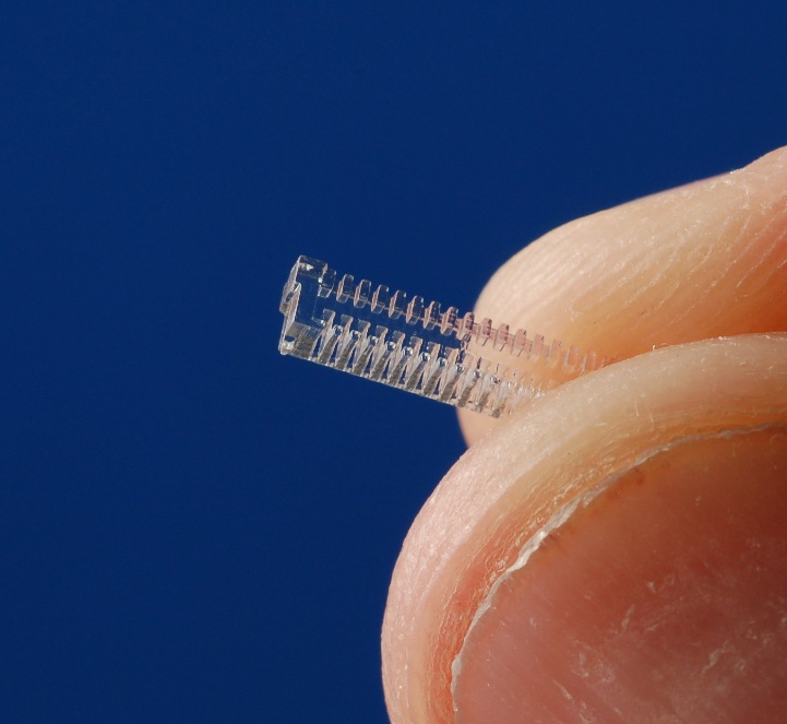
A Medical 16-Conductor Micro Connector
Photo courtesy FineLine Prototyping
Following, we look at some of the players in this field. (Some portions of semiconductor manufacturing and nanotechnology manufacturing are additive as well, but we will not be covering them here.)
Hong Kong Productivity Council (Hong Kong)

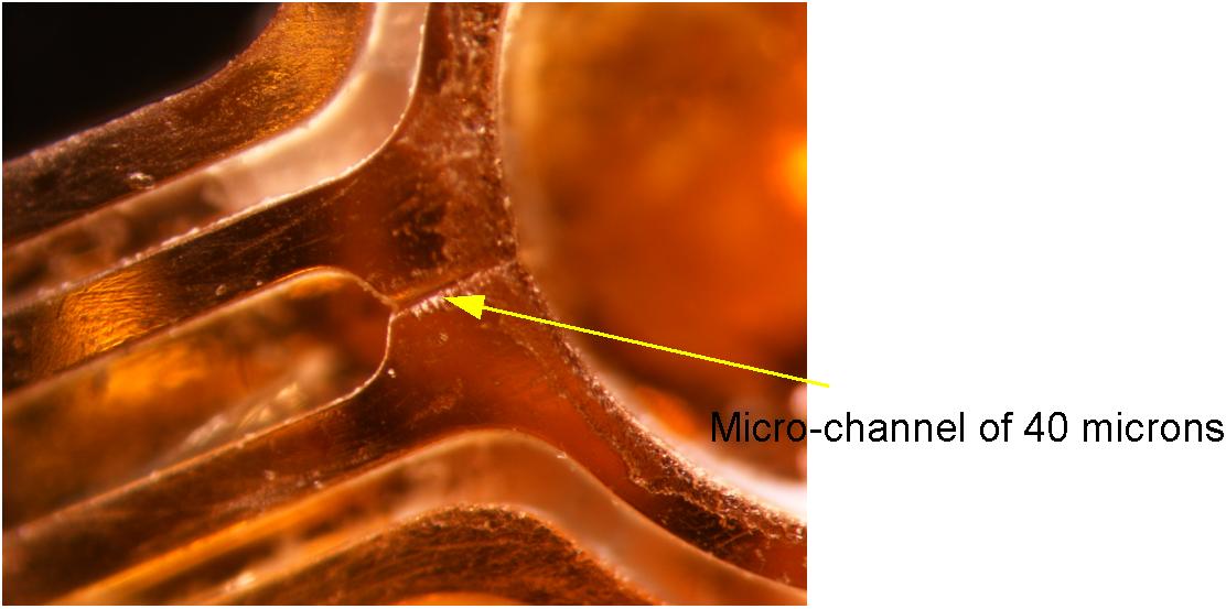
Micro-Channel in a Microfluidic
Photo Courtesy Hong Kong Productivity Council
Micro Fabrication Technology Centre has developed a micro rapid prototyping system based on Digital Light Processing. Resolution is 5-10 microns. Material is acrylate-based resin developed by EPFL. Will run small batch production or sell or license the technology.
Developed jointly by Laser Solutions and JSR, ACCULAS SI-C1000 Micro Laser Modeling System utilizes micro-stereolithography to make parts with resolution of about 1 micron.
3D-Micromac AG (Germany)
Distributed through EOS Group, the microFORM workstation uses selective laser sintering (SLS) under vacuum conditions to form micro metal parts.
Developed in partnership with EPFL, microstereolithography machine uses a DLP-Chip to expose an entire layer at once. Ten micron resolution is possible.
Conducts research on novel micro-scale maskless rapid prototyping technologies
Uses micro laser sintering for the production of metallic and ceramic precision prototypes.